in CO and Architecture edited by
24,099 views
55 votes
55 votes

Consider the following data path of a $\text{CPU}.$

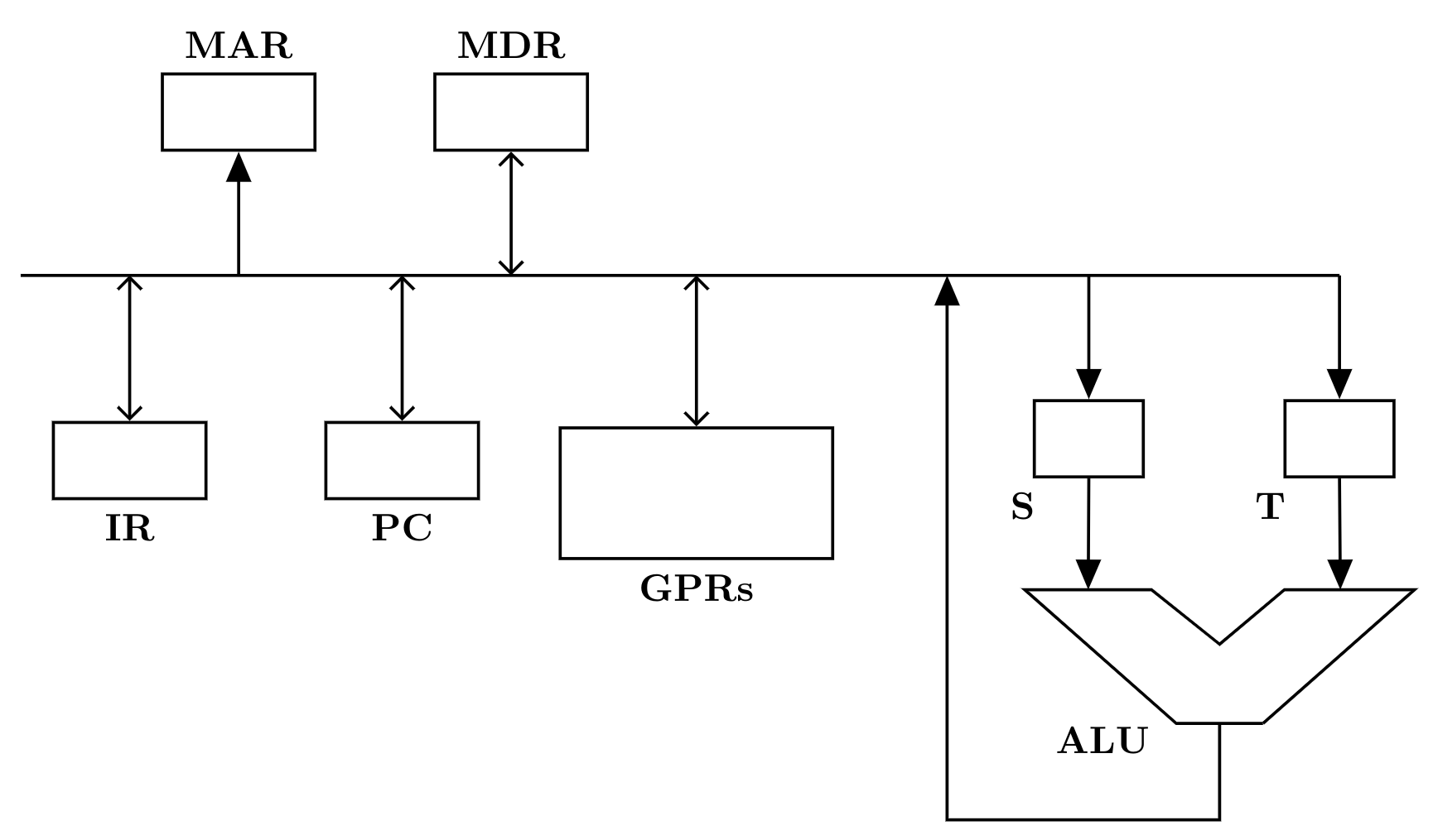
The $\text{ALU},$ the bus and all the registers in the data path are of identical size. All operations including incrementation of the $\text{PC}$ and the $\text{GPRs}$ are to be carried out in the $\text{ALU}.$ Two clock cycles are needed for memory read operation – the first one for loading address in the $\text{MAR}$ and the next one for loading data from the memory bus into the $\text{MDR}.$

The instruction "call Rn, sub” is a two word instruction. Assuming that $\text{PC}$ is incremented during the fetch cycle of the first word of the instruction, its register transfer interpretation is

$\text{Rn} \leftarrow \text{PC} + 1$;

$\text{PC} \leftarrow \text{M[PC]}$;

The minimum number of CPU clock cycles needed during the execution cycle of this instruction is:

  1. $2$
  2. $3$
  3. $4$
  4. $5$
in CO and Architecture edited by
24.1k views

4 Comments

@srestha

Does they asked for it?

Even if they didn't ask then how are you planning to do it ?

They asked to show the execute cycle of "call Rn, sub”.

And that maynot even require PC,GPR,S or T(as shown in diagram) , those thing when this subroutine is calling.

Please, can you write down the steps for $"call\ Rn,sub"$ which you think is valid.

0
0

@Kushagra गुप्ता

I think like this.

Though the question is asking for execution cycle, but in this subroutine call instruction, there is nothing to execute. Like add, subtract or branching like operation. 

So, what is need to be perform here, nothing but Fetch cycle.

Steps are

1) First Fetch address of the subroutine. Put MAR value in PC.

2)Increment PC value. As it is a memory read operation, wait for Memory Function Complete Signal(WMFC).

3) Fetch data By MDR and put it in IR.

Let me know, if it is correct.

0
0
someone please provide video lecture link related to this concept
0
0

12 Answers

87 votes
87 votes
Best answer
  • $\text{MAR} \leftarrow  \text{PC}\qquad \to1$ cycle
  • $S \leftarrow \text{PC}$ (Since these two actions are independent they can be done in same cycle)
  • $\text{MDR} \leftarrow \text{M[MAR]}\qquad \to 2^{nd}$ cycle (System BUS)
  • $\text{Rn} \leftarrow S +1$ $(\text{ALU}$ Is free and the two actions are independent.) (Internal BUS)
  • $\text{PC} \leftarrow \text{MDR}\qquad \to 3$rd cycle

Therefore $3$ cycles needed.

A rough sketch:

Correct Answer: B

edited by

4 Comments

during the 2nd cycle , we are using the bus to transfer the result of (PC+1) into Rn.
That’s why we can’t use it to transfer PC← MDR  @Abhrajyoti00

3
3
edited by

No, @Alekhyo Banerjee. That's not the reason. I got it now. 

We could have done $PC <- MDR$ in the same 2nd cycle only, because reg-reg transfer opn takes 1 cycle and we can do many reg-reg transfer opn in 1 cycle. The problem is that in the 2nd cycle there is a operation of $MDR <- M[MAR]$. Till the value comes into $MDR$, how can we store the value of $MDR$ in $PC$? That's the reason why we need to wait more cycle.

0
0
But the question says that the Instruction is of 2 words, so 1st word is fetched during Fetch cycle, and the 2nd word of the instruction is fetched in the Execution cycle (Instruction Decode cycle) isn't it? Then 1 more cycle should be added to 3 cycles (4 cycles in total). Correct me if I am wrong.
0
0
8 votes
8 votes

Rn <= Pc+1

Pc<= M[Pc]

The sequence of instruction take place 


I Cycle : PC out  , Sin , MARin (MAR can be loaded with PCout

II Cycle: S out  , ALUincrement  , Rn in

III Cycle: MDRout  ,   PCin  (MDRout can be performed once MARin has been performed)   therefore 3 cycle required


2 Comments

why we need to store PC value in MAR and Sin??and can we transfer PC content to Sin and MAR in same clock cycle?

Thanks
1
1
Obviously we can store in same clock because once the content of PC is on bus both the registers MAR and S can activate their load input to take the data on the bus.
1
1
6 votes
6 votes

Hi Guys,

Although many people have provided correct answer but It seems people want to see complete picture so just adding this answer.

So Answer is B part.

In above explanation $S$ is a temporary ALU register. Notice data to and from memory comes and goes via MDR that too via separate BUS.

If provided information is not correct then please notify.

4 Comments

@Chhotu ji

can u share the source, from where u given ans?
0
0

can u share the source, from where u given ans?

@srestha ji,

This answer is not available anywhere. I derived it based on whatever is mentioned in question and standard text book.

0
0
very nice explanation...but i have one doubt

the pc will increment to 2 in instruction fetch phase  or it will increment to 2 after instruction decode phase?
0
0

Great solution considering the book Hamacher et al.

A correction by the way, the register Rnin takes input from MARin

1
1
5 votes
5 votes

1)PCout ,MARin,Rin

2)MDRout ,PCin

2 cycles to read

so total 3  cycles

edited by

2 Comments

can you explain your answer somewhat..as i am not able to understand any of the answers.
0
0

@Arjun Sir.

I am getting this. Question says, ”PC is incremented during the fetch cycle of the first word of the instruction”. So increment not needed during execution phase.

Please tell if this is correct or not.

T1: $PC_{OUT}, MAR_{IN}, Rn_{IN}, READ$

T2: $WMFC (i.e. MBR\leftarrow MEMORY)$

T3: $MBR_{OUT}, PC_{IN}$


0
0
Answer:

Related questions